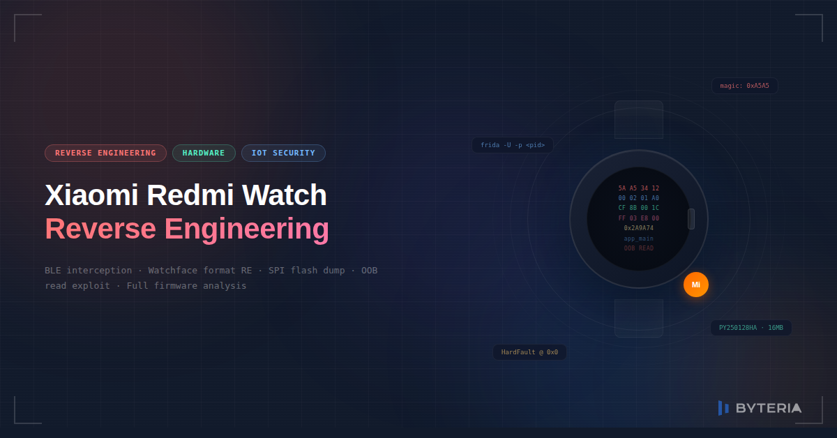

How much security can you expect from a $50 smartwatch? We decided to find out. This is a full technical writeup of our research into the Xiaomi Redmi Watch 5 Active, a SiFli SF32LB551-based wearable that Xiaomi markets as running HyperOS, but under the hood it’s actually RT-Thread (a popular open-source RTOS for embedded systems). Over the course of a week, we intercepted its BLE traffic, reverse-engineered its watchface format, found an out-of-bounds read in the image decoder, desoldered both SPI flash chips, and mapped out the full attack surface.
I wouldn’t call myself a hardware guy, so the physical parts of this project were a bit more time-consuming for me than the software side. But we got through it.
Prerequisites
Before we get into it, here’s what we used:
Software:
– radare2 for static analysis of the 2.8MB ARM Cortex-M33 firmware. We spent days in r2 sessions, and learned the hard way that axt (cross-reference search) is unreliable on large binaries. We ended up tracing function pointer tables manually.
– Frida for hooking the Mi Fitness Android app at runtime, specifically to bypass SSL certificate pinning.
– Mi Fitness, Xiaomi’s companion app. This is where watchface installations are triggered from.
Hardware:
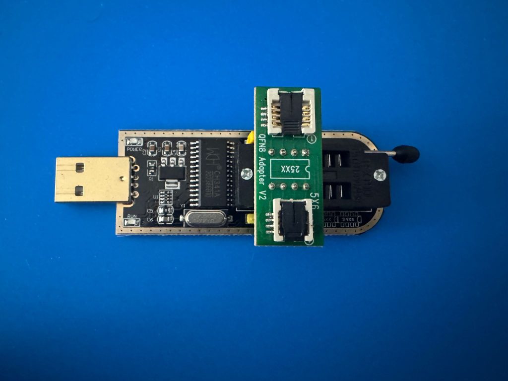
– CH341A Programmer, a cheap USB SPI programmer. Gets the job done.
– QFN8 Adapter for reading the external SPI flash chip after desoldering.
– Soldering iron, solder paste, multimeter for chip removal, reattachment, and not destroying the watch in the process (we succeeded, barely).
– Coffee. Non-negotiable.
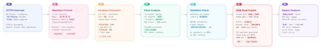
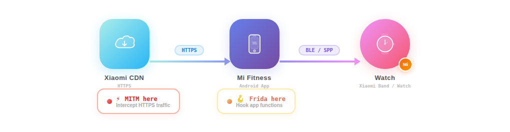
0x00: Intercepting the Traffic
To use the Xiaomi Redmi Watch 5 Active, you need to pair it with your phone through Mi Fitness. Everything goes through this app: watchface management, notifications, health data, firmware updates. The watch itself has no WiFi and no direct internet connection. All data flows through the phone app over BLE.
So our first target was obvious: see what Mi Fitness is actually sending and receiving over the network.
We set up mitmproxy and configured the phone to route through it. As expected, Mi Fitness uses SSL certificate pinning. The app embeds the expected server certificate and rejects anything else, so a simple proxy setup gets you nothing but TLS handshake failures. This is where Frida comes in. We hooked the SSL verification functions at runtime and forced them to return success regardless of the certificate presented. Standard stuff for Android app analysis, but necessary.
With the pinning bypassed, we could see all the HTTPS traffic between Mi Fitness and Xiaomi’s servers. We went through the app feature by feature: health data sync, notification settings, alarm configuration, workout modes, watchface store, firmware updates. Most of these turned out to be simple JSON APIs with nothing particularly interesting. Two features stood out as potential attack surfaces: OTA firmware updates and watchface installations. Both involve pushing binary data to the watch.
We considered looking at the OTA update process first, but there was a practical problem. Firmware updates are a one-shot deal. Once you update, you can’t easily downgrade and repeat the process. Testing would be slow and potentially destructive. Watchface changes are completely reversible. You can install, delete, and reinstall watch faces as many times as you want, which makes them ideal for iterative testing and payload delivery.
So we focused on the watchface pipeline.
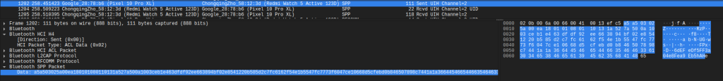
Bluetooth packet capture
Alongside the HTTPS interception, we also captured the Bluetooth traffic between the phone and the watch using Android’s BTSnoop HCI logging (enable it in Developer Options, the logs end up in /data/misc/bluetooth/logs/). We collected three separate captures totaling over 6MB of HCI data and opened them in Wireshark.
From the packet captures, combined with decompiling the Mi Fitness APK (specifically the com.xiaomi.wearable.transport.layerl1 package), we reverse-engineered the transport protocol. The app uses Bluetooth SPP (Serial Port Profile, essentially serial-over-Bluetooth, UUID 00001101-0000-1000-8000-00805F9B34FB) rather than raw GATT writes for bulk data transfer. The protocol has a layered structure:
L1 Packet Format:
+--------+------+-----+--------+-------+---------+
| Magic  | Type | Seq | Length |  CRC  | Payload |
| 2 byte | 1 B  | 1 B | 2 byte | 2 byte| N bytes |
| 0xA5A5 |      |     |  (LE)  | (LE)  |         |
+--------+------+-----+--------+-------+---------+

Types:
  0x00 = NAK (negative acknowledgment)
  0x01 = ACK
  0x02 = CMD (command)
  0x03 = DATA
The CRC is CRC16-CCITT (polynomial 0x1021, init 0xFFFF). We found the exact implementation in the decompiled L1Packet.java:
public class L1Packet {
    public static final short MAGIC = (short) 0xA5A5;
    public static final byte TYPE_NAK = 0;
    public static final byte TYPE_ACK = 1;
    public static final byte TYPE_CMD = 2;
    public static final byte TYPE_DATA = 3;
    // Header: magic(2) + type(1) + seq(1) + len(2) + crc(2) = 8 bytes
}
Watchface transfer flow:
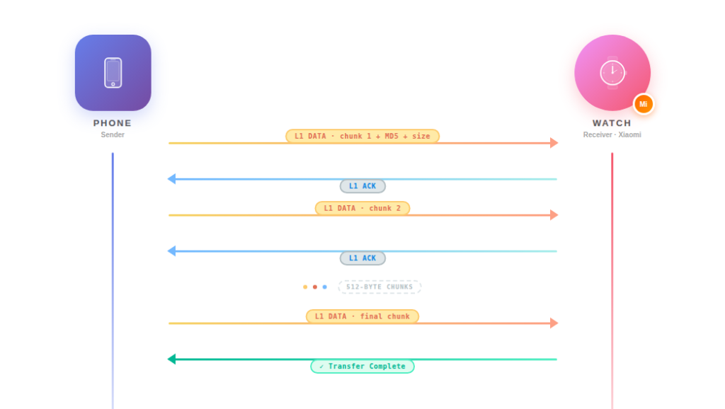
The first chunk includes a 4-byte command header (02 01 27 00), the chunk number, a marker (00 10), the file’s MD5 hash (16 bytes), and the total file size (4 bytes LE), followed by the actual watchface data. Subsequent chunks just carry data.
The important observation here: the transfer protocol has no authentication beyond BLE pairing itself. There’s no session token, no challenge-response, no signing of the transferred data. The watch receives the L1 packets, reassembles the file, checks the MD5 hash for integrity (not security, since MD5 is not a MAC), runs the 4-byte magic check we’ll discuss shortly, and installs the watchface. If you can inject data into this SPP stream, which a MITM position on the HTTPS side allows since you can replace the .bin file before it’s sent over BLE, the watch will accept it.
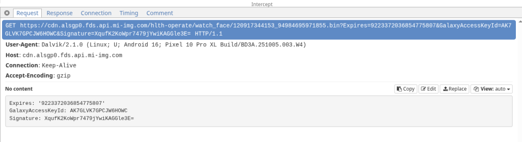
Capturing the watchface binary
When you install a new watch face through Mi Fitness, the app downloads a .bin file from Xiaomi’s CDN (fds.api.mi-img.com) over HTTPS, then pushes it to the watch over BLE using the protocol described above.
We intercepted one of these downloads: 120917344162_102264556486703.bin, 157,196 bytes. A raw binary blob with no obvious file format signature in any public database. Time to open r2.
0x01: The Watchface Binary Format
We had the .bin file. 157,196 bytes, no publicly documented format, no file signature matching anything in binwalk or file magic databases. The only way to understand it was to open it and start reading.
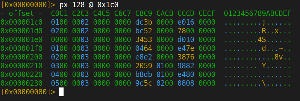
We loaded it into radare2 in 16-bit ARM mode (r2 -a arm -b 16 120917344162_102264556486703.bin) and started with the basics: look at the first few hundred bytes in hex view (px 256).
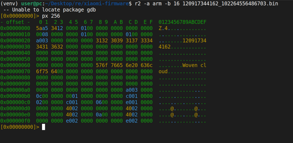
The first four bytes jumped out immediately: 5A A5 34 12. This doesn’t match any standard file format. It’s a proprietary magic value. After the magic, there were some flags, then at offset 0x28 and 0x68, readable ASCII strings appeared: the watchface ID ("120917344162") and the name ("Woven cloud"). That gave us the basic header layout:
Offset  Size  Field               Value
----------------------------------------------
0x00    4     Magic               5A A5 34 12
0x04    4     Flags               00 01 00 00
0x10    4     Data Size           varies
0x14    4     Header/Meta Size    0x000003A0
0x18    4     Resource Count      varies
0x28    64    Watchface ID        ASCII ("120917344162")
0x68    64    Watchface Name      ASCII ("Woven cloud")
At offset 0x1C0, the pattern changed. We saw repeating 16-byte structures with what looked like offsets and sizes. Classic resource table pattern. If you’ve reversed any binary asset format before, this is instantly recognizable. Each entry describes one image or asset in the watchface:
+0x00  4B  Type     (e.g., 0x02000001)
+0x04  4B  Flags    (usually 0x00)
+0x08  4B  Offset   (position in file where data starts)
+0x0C  4B  Size     (data size in bytes)
The next question was: are those offset values absolute memory addresses (like where the firmware maps the file in flash), or are they relative to the file itself? This matters a lot. If they’re file-relative, we can predict exactly where the firmware will read from when processing the file. We checked by adding offset[n] + size[n] for each entry and comparing it to offset[n+1]:
Entry[0]: offset=0x3A0, size=0x16E0 → 0x3A0 + 0x16E0 = 0x1A80
Entry[1]: offset=0x1A80  ✓
Entry[1]: offset=0x1A80, size=0x1BA0 → 0x1A80 + 0x1BA0 = 0x3620
Entry[2]: offset=0x3620  ✓
...contiguous for every single entry.
File-relative. Resources packed back-to-back with zero padding. This means both the Offset and Size fields come directly from the watchface file, so they’re attacker-controlled values. If the firmware trusts them without validation, we have a problem. But to find out, we need the actual firmware binary.
0x02: Hardware
We had the watchface format mapped out and some hypotheses about what happens with those attacker-controlled offset and size values. But to understand what the firmware actually does with them (how it validates, parses, and renders watchface files), we needed the firmware binary itself.
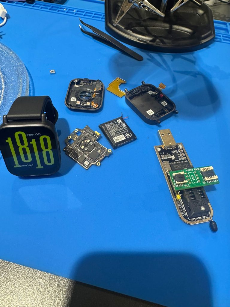
The Redmi Watch 5 Active’s case is sealed with adhesive, no screws. We popped the back cover off with a plastic pry tool and got our first look at the PCB.
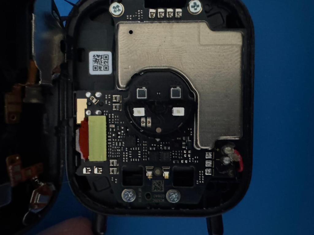
The board is compact. The SiFli SF32LB551 SoC dominates the center, surrounded by a handful of passives and connectors. Our first move was to probe every exposed test pad and connector on the board with a multimeter, looking for anything useful: UART TX/RX, SWD, SPI, whatever. The result was disappointing. We found a single GND pad, and that was it. No debug headers, no labeled test points, nothing that screamed “plug a debugger in here.”
There was, however, one area we couldn’t probe: a yellow metal shield (an RF/EMI can) covering a section of the board. This was the only place where flash chips could be hiding. We heated it up with the soldering iron and carefully lifted the shield off.
Underneath: two PUYA chips.
PUYA Semiconductor is a Chinese fabless company that makes SPI NOR flash memory, the kind of chip you’ll find in basically every budget IoT device and wearable. They’re cheap, small (USON-8 packages, 2x3mm), and supported out of the box by SiFli’s SDK. PUYA’s manufacturer ID is 0x85, and SiFli lists them as a first-tier supported flash vendor alongside GigaDevice and Winbond.
Why two chips? The SF32LB551’s memory architecture uses two separate flash interfaces:
- MPI1 (mapped at
0x10000000): For internal/SiP flash, smaller, used by some chip variants for boot code - MPI2 (mapped at
0x12000000): The main QSPI flash interface. This is where the firmware runs from via XIP (execute-in-place, meaning the CPU fetches and executes instructions directly from flash without copying them to RAM first)
In our watch, the two chips are:
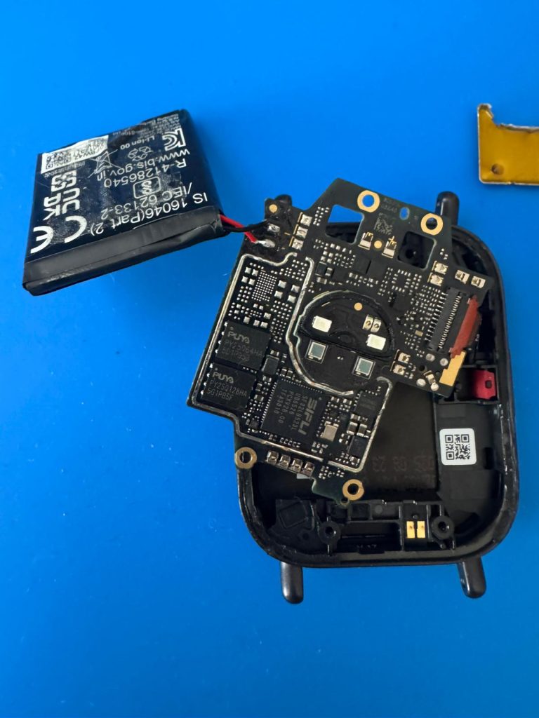
- PY250128HA (128 Mbit / 16MB): The main firmware flash on MPI2. This is where the bootloader,
app_main.bin, UI resources, and user settings live. The CPU executes code directly from this chip via XIP. - PY25064HA (64 Mbit / 8MB): External data storage. Runtime logs, FlashDB key-value database, compressed firmware backup, and BLE bonding data.
We started with the big one. Desoldered the PY250128HA, placed it in the QFN8 adapter, connected to the CH341A, and read the full 16MB. This gave us app_main.bin, the 2.8MB firmware binary that the CPU executes, plus the bootloader, FCES header with the RSA-2048 public key, and all the UI assets.
PY250128HA -- Main Firmware Flash (16 MB)
+--------------------------------------------------+
|  FCES Header + RSA-2048 Public Key (16KB)        |
|  Bootloader (72KB)                               |
|  app_main.bin -- XIP Execute (2.8MB)             |
|  UI images, fonts (9.7MB)                        |
|  User settings, BLE bonds, health data (1MB)     |
+--------------------------------------------------+
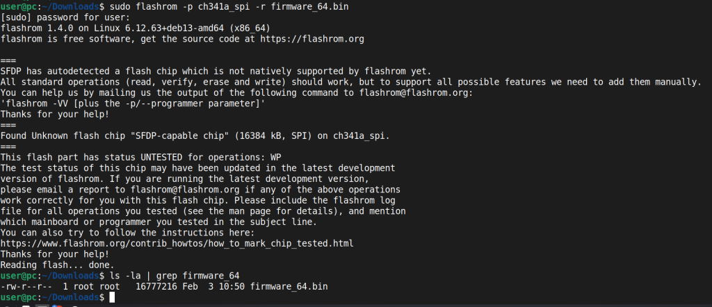
Resoldered it back, then went for the second chip. Desoldered the PY25064HA and read its 8MB:
firmware_mini_chip_32.bin -- 8,388,608 bytes (8 MB)
firmware_64.bin -- 16,777,216 bytes (16 MB)
PY25064HA -- External Data Flash (8 MB)
+--------------------------------------------------+
|  Compressed firmware backup (NOT encrypted)       |
|  FlashDB key-value store (plaintext PII)          |
|  Runtime logs (plaintext)                         |
|  BLE bonding keys (encrypted)                     |
|  Payment tokens (encrypted)                       |
+--------------------------------------------------+
After resoldering both chips back with solder paste, the watch powered on normally. No integrity check on the flash contents at boot, apparently.
0x03: External Flash Analysis
Flash Map
Address Range         Size      Content                    Status
------------------------------------------------------------------------
0x000000 - 0x31D000   3.2 MB    Firmware backup            COMPRESSED (no encryption)
0x352000 - 0x3B4000   401 KB    Resource data              Encoded
0x450000 - 0x470000   128 KB    Runtime system logs        PLAINTEXT
0x541000 - 0x566000   148 KB    FlashDB KV database        PLAINTEXT
0x566000 - 0x596000   192 KB    RT-Thread code + strings   PLAINTEXT
0x5A8000 - 0x5CF000   159 KB    Watchface/icon data        Encoded
The “Encrypted” Firmware Backup That Wasn’t
The first 3.2MB of the flash contains a firmware backup. Our initial entropy analysis at the 256-byte block level showed values of 7.99-8.00, near-maximum entropy, consistent with encryption. We classified it as encrypted and moved on.
Later, we ran a chi-squared goodness-of-fit test. For truly encrypted data (AES, ChaCha, etc.), you expect a chi-squared value around 255 (uniform byte distribution). Our result: 4144. That’s way too high for encryption, but consistent with compression, where certain byte patterns appear more frequently than others even though the overall entropy is high.
We searched for compression signatures and found 219 zlib headers (0x78xx) and 43 gzip headers (0x1F8B). Then we tried raw deflate decompression starting at offset 0x10:
import zlib
data = open("firmware_mini_chip_32.bin", "rb").read()
d = zlib.decompressobj(-15)  # raw deflate, no header
result = d.decompress(data[0x10:])
The first 8 bytes of the decompressed output: SP = 0x2003FA80, Reset = 0x120D3B49. A valid ARM Cortex-M33 vector table, with SP pointing into SRAM and Reset vector in Flash Bank 1 with the Thumb bit set. We compared against app_main.bin and it matched.
The full container format, which we reverse-engineered through trial and error across several iterations:
GLOBAL HEADER (8 bytes):
  [4B] Total decompressed size = 0x00552000 (5,578,752 bytes)
  [4B] Block decompressed size = 0x00002800 (10,240 bytes)

PER-BLOCK (545 blocks):
  [4B] Compressed size (little-endian)
  [4B] Decompressed size (0x2800 for all blocks except possibly the last)
  [raw deflate stream]
We decompressed all 545 blocks. The first 2,834,432 bytes are a 100% byte-for-byte match with app_main.bin. The remaining 2,744,320 bytes are resource data (fonts, icons, watchface assets). Compression ratio: ~57%.
Lesson learned: high entropy does not mean encryption. Always run a chi-squared test. Compression produces entropy around 7.0-7.2 at the 256-byte level with chi-squared ~4000. True encryption produces entropy near 8.0 with chi-squared ~255. We initially got fooled because we were looking at block-level averages that smoothed out the differences.
The security implication is clear: the firmware backup is stored with zero cryptographic protection. Physical access to the SPI flash (or a remote SWD-to-SPI read chain) gives you the complete firmware binary, even if the internal flash uses hardware encryption.
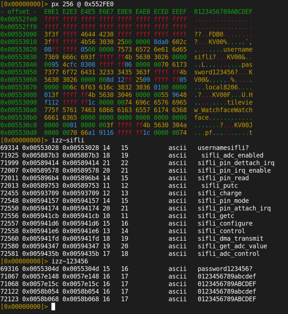
FlashDB: Plaintext Everything
The FlashDB key-value database (a lightweight embedded database commonly used in RT-Thread systems) occupies sectors 0x541000-0x566000. We parsed 65 KV entries across 33 unique keys. The entry format:
[4B status_table][KV00 magic][4B total_len][4B CRC32]
[1B name_status][3B pad][4B value_len][key bytes][value bytes]
Where key_len = total_len - 24 - value_len (the key length is not stored explicitly; you compute it from the total length minus the fixed header overhead minus the value length).
Two entries caught our attention immediately:
username  =  "sifli"
password  =  "123456"

These are SiFli’s SDK default credentials. Left unchanged in production. In plaintext. And this isn’t a one-off. SiFli has a pattern with hardcoded credentials. Their public SDK on GitHub contains a universal bootloader register-lock password 66776677 (hardcoded in #define REG_LOCK_PASSWORD across 8 bootloader projects, same value for every chip family: SF32LB52x, SF32LB55x, SF32LB56x, SF32LB58x). The RT-Thread finsh shell, which is the debug console on these devices, defaults to the password rtthread. It’s default credentials all the way down.
Personal Data at Rest
Data Type        Offset      Value                          Risk
----------------------------------------------------------------------
Phone number     0x4E0DD6    +90534XXXXXXX                  HIGH
Contact name     0x4E0DF7    [REDACTED]                     HIGH
Paired device    0x4F4006    Pixel 10 Pro XL                MEDIUM
Timezone         0x4E2479    Europe/Istanbul                 MEDIUM
Serial number    0x4F5806    6573219263                      HIGH
Quick replies    0x4E367D    "Seni sonra arayacagim"         LOW
SDK creds        0x553010    sifli/123456                    MEDIUM
No encryption. No obfuscation. The only encrypted partitions on the entire flash are upay_safety (payment tokens) and ble (BLE bonding keys: LTK, IRK, CSRK), both protected by the SoC’s hardware crypto engine with keys stored in OTP/eFuse.
0x04: The “Validation”
With the firmware dumped and decompressed, we could return to the original question: does the watch validate incoming watchface files?
The firmware has to validate incoming watchface files somewhere. We searched for the string "watchface" in the firmware binary (/ watchface in r2) and found a format string: "watchface_ota_header_check=%x,%x,%x,%x". The function that references this string lives at 0x2A9A74. This is the validation gate. Whatever this function does determines whether our modified watchface gets accepted or rejected.
Let’s look at it:
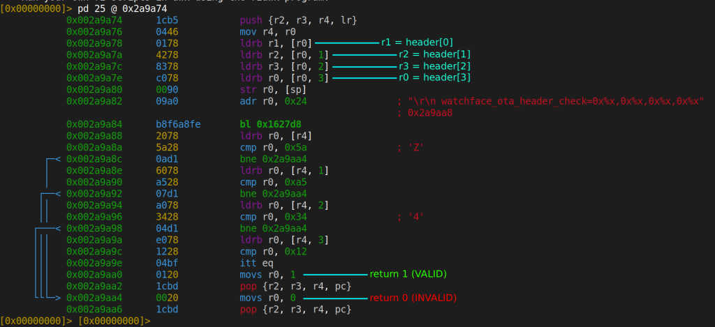
We stared at this for a while, scrolled down looking for the rest of the validation logic, and realized there is no rest. That’s the entire function. Four byte comparisons: [0x5A, 0xA5, 0x34, 0x12]. If those four bytes match, the function returns 1 (valid). That’s it.
No cryptographic signature. No HMAC. No CRC over the file contents. No size validation. No resource table bounds checking. Nothing.
We did find an RSA-2048 public key embedded in the firmware’s FCES header (at the beginning of the flash image), which initially gave us hope that maybe there was signature verification somewhere else. We traced every cross-reference to that key region. It’s used during OTA firmware updates, but never during watchface installation. The watchface path skips it entirely.
To be sure, we fuzzed the magic bytes: we generated 1,020 watchface files, each with a different combination at the first four bytes, and pushed them through the MITM pipeline. Only the exact sequence 5A A5 34 12 is accepted. But once that 4-byte check passes, the firmware blindly trusts everything else in the file: resource offsets, sizes, image dimensions, format bytes. All attacker-controlled. All trusted.
0x05: Out-of-Bounds Read via Image Format Byte
So we can modify any field in the watchface file and the watch will accept it. The question becomes: what can we actually do with that?
The first thing we tried was the obvious: modify the resource table’s Offset field to point outside the file. If the firmware reads from an arbitrary offset without bounds checking, we could potentially read memory that doesn’t belong to the watchface. We tried setting the offset to 0x12000000 (the flash base address) and the watch crashed. Then 0x20000000 (SRAM base), crash again. The firmware was seeking to these addresses but hitting errors before we could see the results.
We stepped back and looked more closely at how the image resources are actually processed. Each image in the watchface has its own small header:
Byte 0:    0x28 (magic)
Byte 1:    format type    <-- this is the interesting one
Byte 2-3:  flags/compression info
Byte 4-5:  width  (16-bit LE)
Byte 6-7:  height (16-bit LE)
Byte 8+:   pixel data
The format byte at position 1 tells the LVGL image decoder which decoding path to use. LVGL is an open-source embedded graphics library, widely used in smartwatches and IoT displays. The format values map directly to LVGL’s lv_img_cf_t enum:
typedef enum {
    LV_IMG_CF_UNKNOWN = 0,
    LV_IMG_CF_RAW,                      /* 1 */
    LV_IMG_CF_RAW_ALPHA,                /* 2 */
    LV_IMG_CF_RAW_CHROMA_KEYED,         /* 3 */
    LV_IMG_CF_TRUE_COLOR,               /* 4 */  ← w * h * 4 bytes (ARGB8888)
    LV_IMG_CF_TRUE_COLOR_ALPHA,         /* 5 */
    LV_IMG_CF_TRUE_COLOR_CHROMA_KEYED,  /* 6 */  ← w * h * 2 bytes (RGB565)
    ...
    LV_IMG_CF_ALPHA_2BIT,               /* 12 */ ← original format in watchface
} lv_img_cf_t;
We found the decoder at lv_img_decoder_built_in_info (0x1F3040) and traced its format handling:
| Format | LVGL Enum | Behavior |
|---|---|---|
0x0C | LV_IMG_CF_ALPHA_2BIT (or SiFli custom LZ) | Reads compressed_size bytes from the buffer. Safe. |
0x06 | LV_IMG_CF_TRUE_COLOR_CHROMA_KEYED | Reads width * height * 2 bytes directly as pixel data. |
0x04 | LV_IMG_CF_TRUE_COLOR | Reads width * height * 4 bytes directly as pixel data. |
Here’s the vulnerability. The firmware allocates a buffer based on the Size field from the resource table (this is the compressed data size in the file). Then it calls the decoder. If the format byte says 0x0C (compressed), the decoder reads exactly the compressed amount. No problem. But what if we flip the format byte from 0x0C to 0x06?
The decoder switches to raw RGB565 mode. It reads width * height * 2 bytes, regardless of how big the buffer actually is. The buffer was allocated for the compressed size, but the decoder reads the uncompressed size.
For a 320×385 image:
Original:  format=0x0C, compressed to 5,856 bytes
Modified:  format=0x06, expects 320 * 385 * 2 = 246,400 bytes raw

Buffer allocated: 5,856 bytes (from resource table Size field)
Decoder reads:    246,400 bytes

OOB read: 246,400 - 5,856 = 240,544 bytes past the buffer
That’s 240KB of memory read past the end of the buffer. Format 0x04 (ARGB8888, 4 bytes per pixel) doubles it: 320 * 385 * 4 = 492,800 bytes, giving nearly 487KB of OOB read. And the data that gets read? It’s displayed on the watch screen as pixels. The watch renders whatever memory contents follow the buffer as an image.
Neither lv_img_decoder_built_in_info at 0x1F3040 nor lv_img_decoder_open at 0x1F3637 performs any bounds check against the allocated buffer size before reading.
Building the exploit pipeline
Changing one byte in a hex editor is fine for a proof of concept, but we wanted systematic coverage. We wrote two tools:
oob_read_exploit.py takes our captured reference watchface as a template and generates modified versions. For each payload, it takes the original file, modifies the first resource entry’s offset and size fields in the resource table, and optionally flips the format byte. The key function is simple: write the target address into the resource table’s offset field at position 0x1C8 (that’s 0x1C0 base + 0x08 offset within the entry), set the size, and save. The watchface magic stays 5A A5 34 12, so the validation passes.
We generated 127 payloads total: – 15 targeted payloads for specific memory regions: RSA public key (0x12000100), FCES header (0x12000000), bootloader vector table (0x12004000), SRAM stack (0x2003E000), BLE state (0x20020000), OTA state structure (0x6039E460), and more – 64 SRAM sweep payloads covering the entire 256KB SRAM (0x20000000 to 0x2003FFFF) in 4KB chunks – 48 flash sweep payloads covering the flash header and bootloader region (0x12000000 to 0x12030000) in 4KB chunks
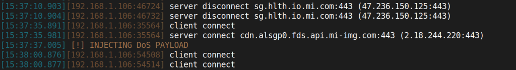
mitm_oob_inject.py is a mitmproxy addon that sits between the phone and Xiaomi’s CDN. When it sees the phone downloading a watchface .bin file from fds.api.mi-img.com, it saves the original response and replaces the body with our crafted payload. It supports single-shot mode (replace with one specific payload) and sweep mode, where every time Mi Fitness downloads a watchface, it uses the next payload in the sequence. Install, screenshot, delete, install again, screenshot, repeat. 64 SRAM addresses in 64 installations.
mitmproxy -s poc/mitm_oob_inject.py                     # default payload
OOB_TARGET=sram_stack mitmproxy -s poc/mitm_oob_inject.py  # target stack
OOB_MODE=sweep OOB_SWEEP=sram mitmproxy -s poc/mitm_oob_inject.py  # sweep
Results on real hardware
We pushed these through the MITM pipeline and installed them on the actual watch. Here’s what we got:
Test Format Buffer OOB Read Result
---------------------------------------------------------------
fmt_0x06 0x06 141KB ~105KB GREEN background + noise at top
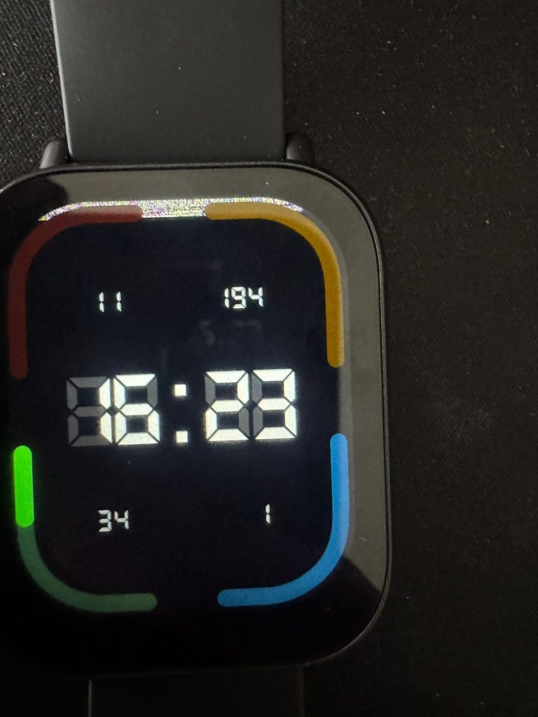
oob_sz50k 0x06 50KB ~196KB BLACK background + noise at top
oob_sz30k 0x06 30KB ~216KB BLACK background + noise at top
oob_sz10k 0x06 10KB ~236KB REBOOT (HardFault)
fmt04_max 0x04 141KB ~351KB REBOOT (read too large)
fmt04_sz50k 0x04 50KB ~442KB BLACK + noise
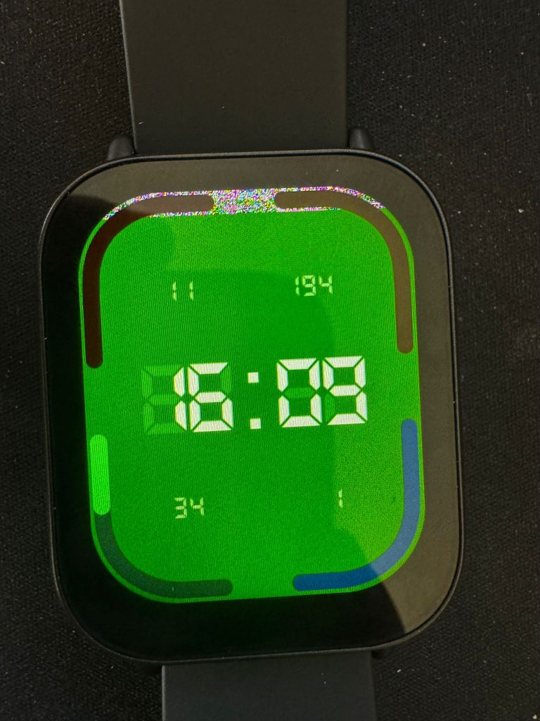
The green background in the large-buffer test is significant: 0x07E0 in RGB565 is pure green, which is the chroma key transparency color. This means the decoder is reading past the buffer into adjacent flash/file data and displaying it as pixels. Those noise pixels at the top? That’s actual memory content being rendered as an image.
The black background in the smaller-buffer tests tells us something important: the heap is zeroed after free. OOB reads into heap territory return 0x0000, which is black in RGB565. The watch effectively hides its own vulnerability by being boring. You can read 200KB past the buffer, but most of it comes back as black pixels because the heap allocator zeros freed memory.
The 10KB test crashes the watch entirely. At that OOB range (~236KB), the read crosses the 256KB SRAM boundary (0x20000000-0x2003FFFF) and hits unmapped memory, triggering a HardFault exception and an immediate reboot.
What could you actually leak?
In theory, the OOB read can access anything mapped in the CPU’s address space: flash, SRAM, peripheral registers. In practice, the zeroed heap limits what’s useful. The most interesting data would be SRAM globals (BLE connection state, crypto keys in memory during active sessions) or flash contents (firmware code, embedded keys). But extracting usable data from watch-screen pixels requires photographing the display and converting RGB565 values back to bytes, not exactly efficient for large-scale exfiltration. It’s a real vulnerability, but an impractical one for data theft. The DoS angle (crashing the watch) is more immediately exploitable.
One important note: the OOB read operates on SRAM heap memory (0x20000000 range). The FlashDB data we found in the flash analysis (0x03) lives on the external SPI flash, accessed through the SPI controller, a completely different address space. There’s no direct path from this vulnerability to that data.
Integer overflow in bounds checking
We also found an integer overflow bypass. The firmware performs a sanity check on resource offsets: offset + size <= file_size. But it uses unsigned 32-bit arithmetic:
offset = 0xFFFFFFF0 (from resource table)
size = 0x00000020
Check: 0xFFFFFFF0 + 0x20 = 0x00000010 (uint32 wrap)
0x10 &lt;= 157,196 --&gt; PASSES
Result: firmware seeks to offset 0xFFFFFFF0 --> unmapped memory --> crash
The overflow bypasses the bounds check, but the resulting address contains no valid image header, so it crashes rather than producing controlled output. Still, it’s a clean DoS vector and demonstrates the complete absence of robust input validation.
0x06: Deeper Firmware Analysis
After decompressing the firmware backup, we had a 5.6MB image containing both code and resources. This gave us access to data that wasn’t present in the app_main.bin dump alone.
It’s a debug build
At offset 0x0017D474:
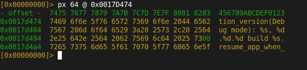
solution_version(Debug mode): %s, %d.%d.%d build %s
And the boot banner at 0x00524440:
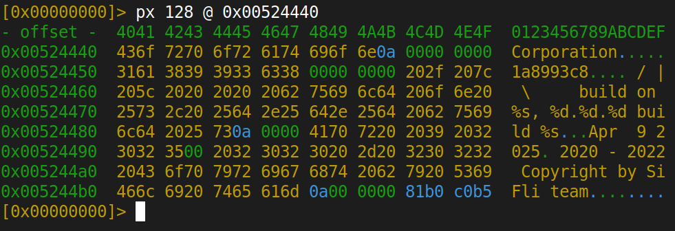
 \ | /
S. - SiFli Corporation
    1a8993c8
 / | \     build on %s, %d.%d.%d build %s
Apr  9 2025
The production firmware shipped to retail devices is compiled in debug mode. SiFli SDK version 1.0.9, git commit 1a8993c8, built April 9, 2025. Debug builds typically include verbose logging, active test interfaces, and relaxed security checks.
Cryptographic keys in format strings
At offset 0x004225B3:
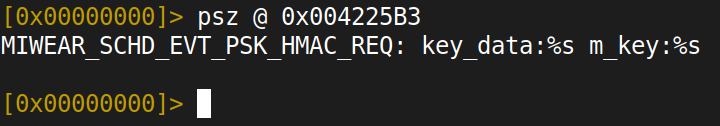
MIWEAR_SCHD_EVT_PSK_HMAC_REQ: key_data:%s m_key:%s
This format string is designed to print the HMAC key data and the master key as plaintext strings. Given that this is a debug build, these strings would be emitted to the debug UART during the PSK binding process. We haven’t captured UART output during pairing to confirm this, but the format string’s intent is unambiguous.
The binding protocol itself uses a reasonable cryptographic stack: ECDH for key agreement, HKDF-SHA256 for key derivation, HMAC-SHA256 for mutual verification, and AES-128-CCM for session encryption. The derived keys include token_key, beacon_key, device_key, and separate session_key.dev_key/session_key.app_key for bidirectional communication. But logging the intermediate key material over UART undermines all of it.
Phone/PC unlock mechanism
The firmware implements a mechanism to unlock Xiaomi phones and PCs from the watch. We identified this through error strings in the binary:
[E] UNLOCK: aes128 encrypt failed, error %ld
[E] UNLOCK: %s AUTHORIZE, expect len %d, got %d
[E] UNLOCK: %s AUTHENTICATE, expect len %d, got %d
Functions miwear_unlock_phone_info and miwear_unlock_pc_info handle the token exchange using AES-128 encryption. This is a legitimate feature (Xiaomi phones support unlocking via paired wearables), but it means a compromised watch could potentially serve as an escalation path to the paired phone. We haven’t tested this scenario.
0x07: Static Analysis
Beyond the watchface vulnerability, the firmware binary reveals a broader attack surface. Everything in this section comes from static analysis of app_main.bin using radare2: tracing function calls, reading disassembly, and following string references. We haven’t tested these findings live over BLE yet, but the code is clear enough to draw conclusions.
The watch runs SiFli’s SIBLES stack, built on top of the Riviera Waves (RW) BLE implementation. We identified 12 distinct GATT services by tracing registration functions and string references in r2. Most are standard: heart rate, notifications, time sync. But one stood out.
DLVP: Debug Lever Via Protocol
DLVP is SiFli’s settings protocol, exposed over BLE GATT handles 0xA407 through 0xA40E. Among the settings it controls is one called jlink_uart_switch. The function that handles it lives at 0x0FC208:
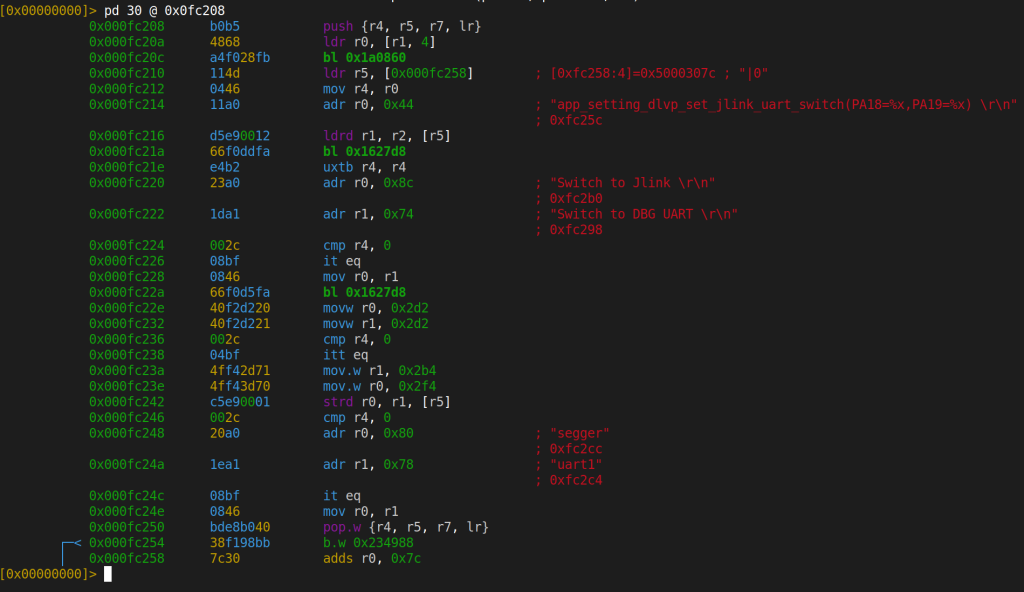
This function reconfigures GPIO pins PA18 and PA19 by writing to the pinmux register at 0x5000307C. When the flag is non-zero, the pins are set to 0x2D2/0x2D2, which is JTAG/SWD mode. When zero, they’re set to 0x2F4/0x2B4, which is debug UART mode.
| Mode | PA18 | PA19 | Effect |
|---|---|---|---|
| JTAG/SWD | 0x2D2 | 0x2D2 | Debug port OPEN |
| DBG UART | 0x2F4 | 0x2B4 | Debug UART OPEN |
The call chain from BLE to this function:
BLE GATT Write Event
  --> 0x0FBD84 (DLVP packet dispatcher)
    --> RAM callback table [0x60398D9C]
      --> 0x0FC208 (jlink_uart_switch)
        --> GPIO 0x5000307C write
        --> 0x234988 (persist to flash + notify)
In the static analysis, we could not identify any authentication check in the dispatch chain between the GATT write handler and the GPIO reconfiguration. If this works as the code suggests (and we haven’t tested it live yet), you’d write a value to a GATT characteristic from your phone using nRF Connect, and the watch would reconfigure its debug port pins. The setting even persists to flash.
One note: the GATT UUIDs for the DLVP service are constructed dynamically in RAM at runtime. They don’t appear as static constants in the binary. You’d need to do a live BLE scan (e.g., with nRF Connect) to discover the exact characteristic UUIDs.
212 Shell Commands
We initially found 41 debug shell commands registered in resources.bin at offset 0x1C13F8 (12 bytes per entry: [name_ptr][desc_ptr][handler_ptr]). After deeper analysis of the decompressed firmware’s resource section, that number jumped to 212. Some highlights:
| Command | What it does |
|---|---|
forget_pwd | Bypass/reset the device PIN |
get_reset_key | Retrieve the PIN reset key |
write_efuse_uid | Write to eFuse. This is one-time programmable and irreversible |
read_efuse_uid | Read eFuse UID |
regop | Arbitrary register read/write |
flash | Raw flash read/write |
bt_hci | Direct HCI command injection |
dbguart2jlink | Same JTAG switch we found via DLVP |
kvdb_reset | Wipe the key-value database |
The write_efuse_uid command is particularly notable. eFuse bits are one-time programmable. Once written, they cannot be unwritten. This command is registered in the debug shell, which is reachable via UART (confirmed by string references). Whether these commands are also reachable via BLE SPP would require live testing to confirm.
BT CLI
The BT command handler at 0x0F4838 uses a strcmp dispatch chain to process commands:
0x0F4848  adr r1, "delbond"
0x0F484C  bl 0x1A1BF8            ; strcmp(input, "delbond")
0x0F4850  cbz r0, handler        ; match --> delete bonding info
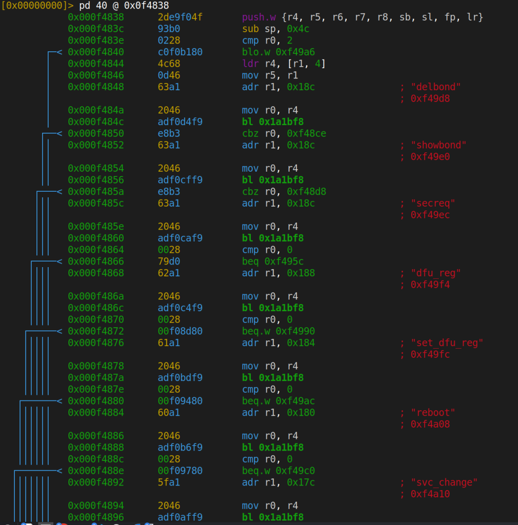
Commands we identified in the dispatch chain include delbond (delete BT bonding), showbond (dump paired device list), reboot, dfu_reg (read DFU register), and set_dfu_reg (write DFU register). All identified through static analysis.
We also found a factory mode entry point (0x107BB8) triggered by sending byte 0x40 (‘@’) over UART, and a BQB test mode (0x0642DC) that appears to disable BT security controls for RF qualification testing. Both are compiled into the production firmware binary.
The command dispatcher at 0x074A00 (~7KB of dispatch logic) includes CMD_GO_TO_flash_write, a raw flash write command. Again, present in the production binary.
0x08: Attack Chains
Individually, some of these findings might seem minor. Combined, they enable several complete attack scenarios:
Scenario 1: MITM Watchface Injection (confirmed)
Attacker (on network) --> MITM Mi Fitness HTTPS --> Replace .bin --> OOB Read / DoS
Requires a MITM position between the phone and Xiaomi’s CDN, plus an SSL pinning bypass on the Mi Fitness app (or root access to the phone). We confirmed this works: the watch accepts any watchface with the correct 4-byte magic, no signature check.
Scenario 2: BLE to Full Debug Access (code analysis only, not tested)
nRF Connect --> GATT Write (DLVP) --> SWD enabled --> J-Link --> Full control
The code for this exists and the logic is straightforward, but we haven’t tested it live over BLE. If it works as the disassembly suggests, it would be the most concerning scenario: within BLE range, no physical contact required.
Scenario 3: Physical Flash Dump (confirmed)
Open watch --> Desolder SPI flash --> CH341A --> All data
We did this. Requires physical access. Yields all plaintext data: contacts, phone numbers, paired devices, SDK credentials, full decompressed firmware.
ROP gadget availability
If an attacker achieves controlled code execution (e.g., through a more sophisticated exploitation of the OOB read or the integer overflow), the 2.8MB firmware provides ample ROP material:
- 29,550
pop {pc}gadgets - 20,778 indirect branches (
bx/blx) - Stack pivot:
mov sp, r7; pop {r7, pc}at0x0038B8 - Memory write:
str r6, [r0, #4]; pop {r1, r7, pc}at0x02B921 - LVGL multiplication-to-malloc chains at
0x160EC0with integer overflow risk
0x09: Vulnerabilities
Here’s what we actually found and confirmed:
Watchface exploit (confirmed on device):
- OOB Read via image format byte. Flipping one byte in the resource table makes the LVGL decoder read past the buffer. We tested 127 payloads, observed green and black screens depending on memory region.
- No watchface signature verification. The only check is a 4-byte magic number. Modified watchfaces are accepted and rendered without question.
- Integer overflow in resource bounds check. Crafting resource sizes that wrap around uint32 triggers a reboot.
- DoS via malformed watchface. Multiple crash vectors found. The watch reboots and falls back to the default face.
Flash dump findings (confirmed via physical extraction):
- Plaintext PII in external flash. Phone numbers, contacts, and paired device info sitting in the clear on the SPI flash.
- SDK default credentials in FlashDB.
sifli/123456stored as plaintext key-value pairs. - Plaintext runtime logs in external flash. System logs readable directly from the flash dump.
- Unencrypted firmware backup. The compressed backup decompresses to a byte-for-byte match with app_main.bin. No encryption, just deflate.
- Debug build on a production device. The firmware literally contains the string “Debug mode” in its version banner.
0x0A: Closing Thoughts
We spent a week on this watch. Thousands of instructions read in r2, Frida scripts written and rewritten, a flash chip desoldered and (successfully) resoldered, 127 OOB payloads crafted, 545 deflate blocks individually decompressed, and FlashDB entries parsed by hand until we got the format right.
The watchface exploit chain is real and confirmed: a 4-byte magic check as the only validation, an image decoder with no bounds checking, and a MITM pipeline that lets you inject arbitrary payloads during installation. The flash dump tells the rest of the story: plaintext PII, default SDK credentials, unencrypted firmware backups, and a debug build running on a production device.
The static analysis findings (JTAG over BLE, 212 shell commands, phone unlock mechanism) are interesting leads, but we haven’t tested them live. That’s a project for another day.
We did, however, manage to break half the display in the process. The screen only works on one side now. Worth it.
As for responsible disclosure: I did try to go through the bug bounty process before publishing this. After a week with no response, I decided to publish. I hate procedural stuff. Building things in the open is more fun anyway.
Thanks to Selim Can Ozdemir and H. Utku Altunok for their help during this research.
All research materials, tools, and payloads used in this project are available at https://github.com/Byterialab/xiaomi-smart-watch-research.
https://github.com/lvgl/lvgl
https://github.com/OpenSiFli/SiFli-SDK
https://github.com/armink/FlashDB
